Conductive paths and layers
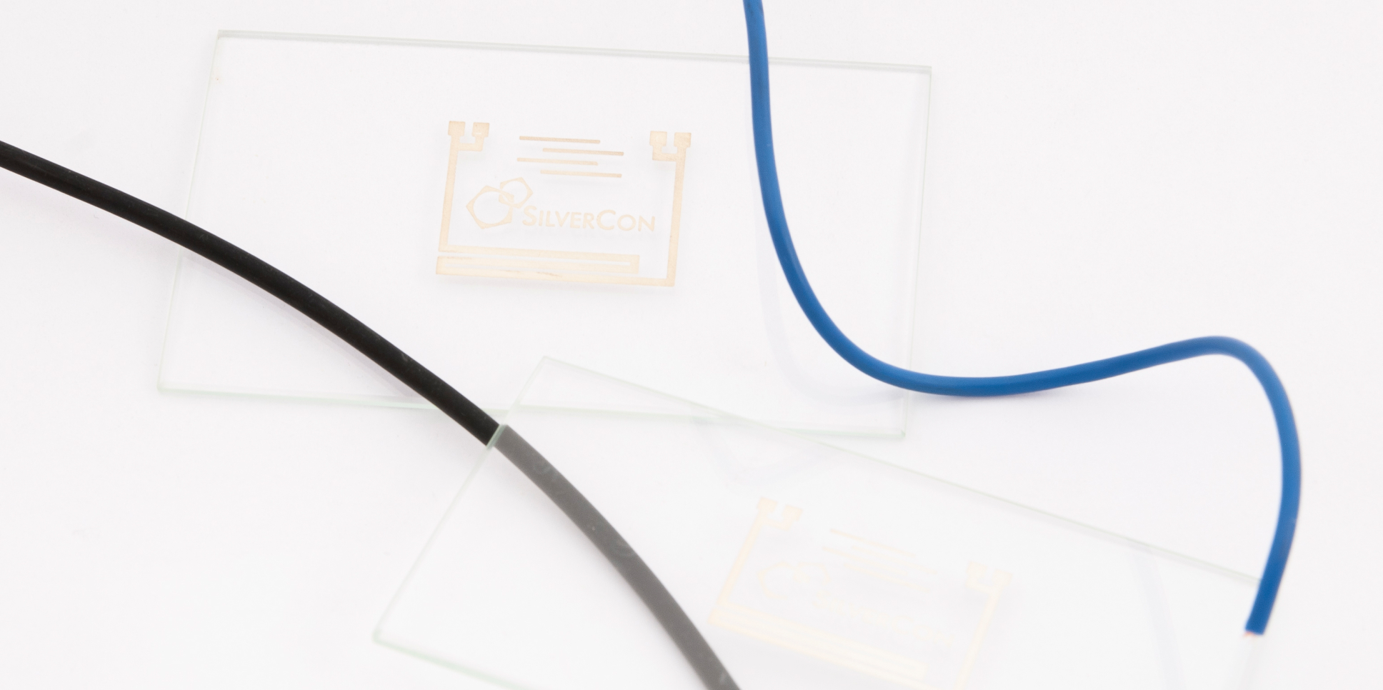
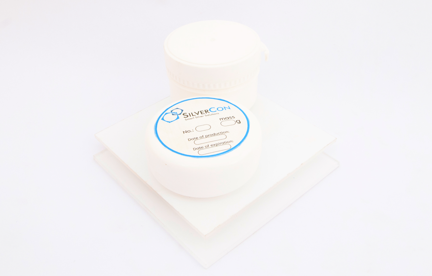
Inks and pastes are primarily used in our coating processes, therefore they can be widely used in printed electronics. The great advantage of our technology is the possibility to obtain layers as thick as 0.5-5µm. High surface adhesion and low temperature sintering allows our solutions to be used on bendable materials, such as foil, paper, or fabrics. Inks and pastes can be applied with screen printing, offset, stamping and many more methods.


Get to know our process
Products: pastes, inks
Materials: copper, aluminium, thermosensitive materials, ceramics
Stage 1
Nanoszenie kompozytu
The composite can be applied partially or to the whole surface using any available method, according to customer needs.
Stage 2
Sitodruk
The layer is being sintered using on of the available methods. Prefered method depends the scale and specific requirements of the order.
Obtained layer
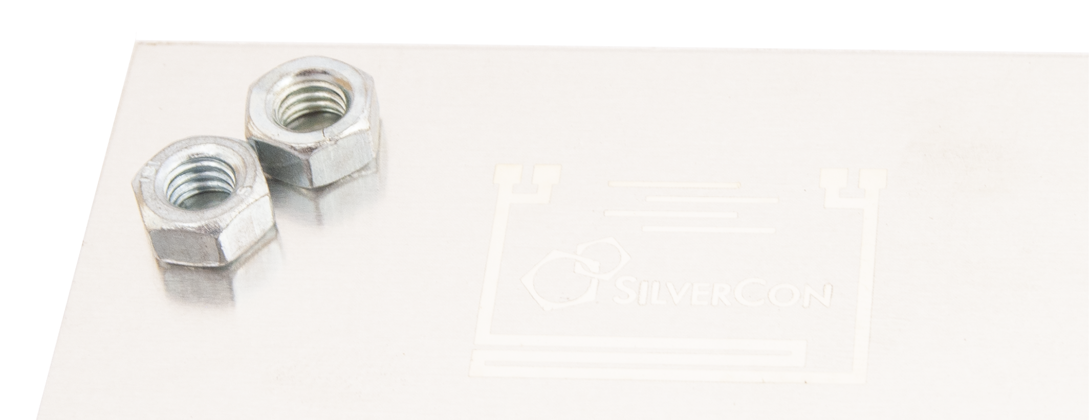
As a result the surface is covered with high-quality coating that has defined characteristics and properties.

Ask for a quote
Drop us your e-mail address and we will contact you